Organic Field Effect Transistors (OFETs)
The interest for Organic Field Effect Transistors (OFETs) has drastically increased over the past few years, and they have been intensively studied for many applications such as displays, smart tags and sensors. The reason for focused research interest in the field of “plastic electronics” is the opportunity to produce low cost devices on plastic substrates on large areas, opening, indeed, an entire new market segment.
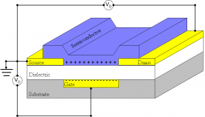
OFETs are close relatives of the classic Metal Oxide Semiconductor Field Effect Transistors (MOSFETs); typically, since the organic semiconductors are characterized by a low conductivity if compared to inorganic ones, Thin Film Transistor (TFT) architecture is preferred in this case. The core of an OFET is a Metal-Insulator-Semiconductor structure (MIS), which can in principle be considered as a parallel plate capacitor: the two capacitor plates are formed by a metal electrode, called gate electrode, and a semiconductor, which are separated by a thin insulating film, called gate dielectric. Two additional electrodes, called Source and Drain electrodes are patterned in order to contact the organic semiconductor allowing probing the conduction across the organic film.
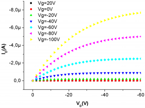
One of the main differences between an OFET and the classic MOSFET is that while the latter typically works in inversion mode, OFETs usually work in accumulation mode. When a negative (positive) voltage is applied between the gate and the source electrodes, an electric field is induced in the semiconductor that attracts positive (negative) charge carriers at the semiconductor/insulator interface between source and drain electrode and overlapping with the gate. Applying a negative (positive) voltage between source and drain electrodes, it is possible to drive the positive (negative) charge carriers across the channel area. Upon increasing gate voltage to positive (negative) values, the number of charge carriers accumulated in the channel will reduce until the channel is fully depleted of free carriers. Below the threshold voltage the device is in its off state, no free charge carriers are present in the channel and no current will flow across it. The equations that govern the OFET working principle are substantially the same of the classic MOSFET. When a gate voltage larger than the threshold voltage is applied, with a small applied source drain voltage, the gate induced field is almost uniformly distributed along the conducting channel, thus a uniform charge distribution is induced in the channel. The device is operating in the linear region. For larger drain voltages, the gate field at the drain contact is zero. As a result, a depleted area with no induced free charge carriers is present. This phenomenon is called pinch-off. Beyond this point the current flowing across the channel saturates and a further increase in the applied source/drain voltage will produce no significant effects on the measured current.

